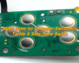
A PCB pad for metal dome is the contact area on a PCB that allows a metal dome to close a circuit when pressed. The pad design affects contact stability, tactile feedback, assembly accuracy, and switch life. For products such as control panels, handheld devices, medical keypads, industrial interfaces, metal dome keyboards, and membrane dome switch assemblies, the PCB pad should be planned before tooling and mass production.

A metal dome switch works as a complete structure, not as a single part. The dome, PCB pad dimensions, surface finish, adhesive spacer, actuator, overlay, and assembly method must match each other. When these details are controlled, the switch can provide stable electrical response and consistent tactile feedback.
EBest Circuit supports PCB pad for metal dome review, metal dome array structure, dome selection, and custom keypad assembly. This helps customers reduce prototype changes and improve production consistency.
What Is a PCB Pad for Metal Dome?
A PCB pad for metal dome is a copper contact pattern designed on a printed circuit board. It normally includes an outer pad and an inner pad. The metal dome sits above these contact areas. When pressed, the dome center touches the inner pad and connects it with the outer pad, creating a momentary switch signal.
The outer pad supports the edge of the metal dome. The inner pad receives the contact from the dome center. A clear gap between these two areas keeps the circuit open before actuation. This structure is widely used in snap dome switches because it combines electrical switching with tactile feedback.
The PCB metal pad can be round, oval, cross-shaped, ring-shaped, or customized based on the dome type and product layout. Round metal domes usually use a center pad and a ring-shaped outer pad. Other dome shapes may require different pad structures.
A PCB pad board for metal dome use should consider the dome diameter, actuation force, solder mask opening, surface finish, adhesive layer, and actuator position. These factors affect how the dome sits, moves, and contacts the PCB.
How Does a Metal Dome Work on a PCB Pad?
A metal dome works as a spring contact on the PCB pad. In the normal position, the dome center stays above the inner pad. When pressure is applied, the dome collapses. The center then touches the inner pad and completes the circuit. After the pressure is released, the dome returns to its original shape and opens the circuit again.

The working process includes four basic stages:
- Rest position: The dome is seated above the PCB pad.
- Pressing stage: Force is applied through a key, actuator, or overlay.
- Contact stage: The dome center touches the inner pad and closes the circuit.
- Release stage: The dome returns and the circuit opens.
The PCB pad must support this movement. If the outer pad does not support the dome edge correctly, the dome may tilt or feel uneven. If the inner pad is too small, contact may become less stable. If the gap is too narrow, electrical separation may be affected by process tolerance or contamination.
The actuator should press near the dome center. Off-center pressure can change the snap feel and may reduce contact consistency. A well-matched PCB pad, dome, spacer, and actuator help the switch work predictably.
Why Is PCB Pad Design Important for Metal Dome Switches?
PCB pad design is important because it affects both electrical contact and tactile response. The metal dome provides the snap action, but the pad controls where and how the contact is made. A high-quality dome may still perform poorly if the pad layout is not suitable.
A correct pad design helps improve contact stability, key feel, assembly accuracy, and production yield. It also reduces variation between different keys on the same product. This is important for metal dome keyboards, control panels, handheld devices, and industrial keypads.
The PCB pad also influences inspection and testing. A clear pad structure makes it easier to align the metal dome array and verify key function during production. This improves consistency from prototype to batch production.
| Design Goal | Function |
|---|---|
| Stable electrical contact | Helps the switch trigger clearly when pressed |
| Consistent tactile response | Keeps key feel uniform across the product |
| Proper dome support | Allows the dome to sit flat and move correctly |
| Suitable process tolerance | Reduces assembly and testing variation |
| Longer switch life | Supports repeated pressing with stable performance |
EBest Circuit reviews pad layout together with dome size, force requirement, surface finish, and assembly structure. This helps identify layout issues before tooling or mass production.
What Are the Basic PCB Pad Dimensions for Metal Domes?
Basic PCB pad dimensions depend on the metal dome diameter, shape, force, travel, and product structure. There is no universal size for all snap domes. The pad should be designed according to the selected dome specification.
For a round metal dome, the outer pad usually supports the dome edge, while the inner pad sits at the center. The gap between them keeps the circuit open before pressing. The solder mask opening should expose the correct contact area without reducing insulation.

Common metal dome sizes include 4 mm, 5 mm, 6 mm, 8 mm, 10 mm, and 12 mm. Smaller domes are used in compact electronics. Larger domes are used for stronger tactile response or easier operation.
| Metal Dome Diameter | Typical Inner Pad Diameter | Typical Outer Pad Width | Common Use |
| 4 mm | 1.0–1.5 mm | 0.5–0.8 mm | Small remotes, compact devices |
| 5 mm | 1.5–2.0 mm | 0.6–1.0 mm | Consumer keypads |
| 6 mm | 2.0–2.5 mm | 0.8–1.2 mm | Control buttons |
| 8 mm | 2.5–3.5 mm | 1.0–1.5 mm | Industrial and medical controls |
| 10 mm | 3.0–4.5 mm | 1.2–1.8 mm | Larger keypads |
| 12 mm | 4.0–5.5 mm | 1.5–2.0 mm | High-force buttons |
These values are reference ranges. Final PCB pad dimensions should be confirmed with the dome datasheet, PCB process capability, adhesive structure, and mechanical design.
If the PCB is completed before dome selection, the available pad may limit dome options. It is better to confirm the dome and PCB pad together during the early design stage.
What Gap Is Needed Between the Inner and Outer Pads?
The gap between the inner and outer pads keeps the circuit open before the metal dome is pressed. In many low-voltage metal dome PCB designs, the gap is commonly around 0.2 mm to 0.5 mm. The exact value depends on PCB manufacturing tolerance, dome size, solder mask design, and reliability requirements.
A smaller gap saves space but requires tighter process control. A larger gap improves insulation margin but may reduce available contact area. The best choice is usually a balanced gap that supports both reliable contact and stable insulation.
| Pad Gap Range | Design Effect | Suitable Use |
| 0.15–0.20 mm | Compact layout with tight tolerance control | Space-limited products |
| 0.20–0.35 mm | Balanced contact area and insulation | Common metal dome PCB layouts |
| 0.35–0.50 mm | Higher clearance and process margin | Larger domes or industrial products |
| Above 0.50 mm | More separation but less central pad area | Special or large-size structures |
The solder mask opening should also be controlled. If too much copper is exposed, the dome may contact an unintended area. If the opening is too small, the usable contact area may be reduced.
For critical products, sample testing with different pad gap options can help confirm contact resistance, tactile feel, and assembly stability before final production.
How Does Pad Size Affect Snap Dome Feel?
Pad size affects snap dome feel by changing dome support and contact position. The dome force curve mainly comes from the dome itself, but the PCB pad affects how the dome sits and how it lands during actuation.
A larger outer pad gives the dome edge more support. A smaller outer pad saves space but may reduce stability if it does not match the dome footprint. The outer pad should support the dome edge without interfering with dome movement.
The inner pad affects contact reliability. A larger inner pad gives more contact margin, while a smaller inner pad saves space. However, the inner pad must still provide enough area for stable contact after the dome snaps down.
| Pad Design Factor | Effect on Switch Feel | Recommendation |
| Larger inner pad | More contact margin | Keep enough gap from the outer pad |
| Smaller inner pad | Compact design | Use only when tolerance allows |
| Wider outer pad | Better dome edge support | Match the dome footprint |
| Narrow outer pad | Saves PCB space | Confirm with dome specification |
| Centered pad layout | More consistent tactile response | Align actuator with dome center |
| Uneven pad layout | Less stable key feel | Avoid asymmetric contact areas |
The actuator and spacer also affect snap feel. The actuator should press the dome center, and the spacer should allow the dome to move freely. Pad size should be reviewed together with the full mechanical stack-up.
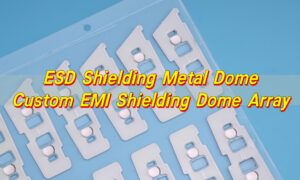
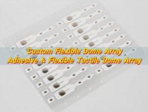
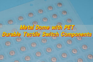
Can a Metal Dome Array Be Mounted Directly on PCB Pads?
Yes, a metal dome array can be mounted directly on PCB pads if the pad layout, array position, adhesive design, and surface finish are suitable. A metal dome array usually places multiple domes on a PET carrier with adhesive. The array is then laminated onto the PCB so each dome aligns with its matching pad.
This structure is widely used because it simplifies assembly and improves dome positioning. The PCB provides the contact circuit, while the metal dome array provides tactile switching. This design is common in handheld devices, industrial panels, medical equipment, remote controls, and metal dome keyboards.

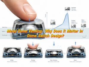
Direct mounting requires accurate alignment. Positioning holes, outlines, fiducials, or tooling marks can help control placement. The adhesive must hold the domes in position without restricting dome movement.
Important design points include:
- Dome-to-pad alignment for stable contact.
- Adhesive selection to keep the array flat.
- Venting path to let air move during pressing.
- Suitable PCB surface finish for stable contact resistance.
- Controlled overlay pressure to avoid restricting the dome.
Surface finish is important for contact performance. ENIG is commonly used because it provides a flat and corrosion-resistant surface. Hard gold may be used for higher durability requirements. HASL may be less suitable for precise tactile contact because its surface is not as flat.
EBest Circuit can support direct-mounted metal dome array projects by reviewing PCB pad layout, dome type, adhesive stack-up, and surface finish before production.
How Is a Metal Dome Keyboard Designed on a PCB?
A metal dome keyboard on a PCB is designed by combining PCB contact pads, circuit routing, metal domes, adhesive layers, and a top interface layer. The PCB carries the electrical circuit. The metal domes provide tactile switching. The overlay, keycap, or actuator transfers finger pressure to the dome.
The design usually starts with the keypad layout. Key quantity, key spacing, dome size, actuation force, connector position, backlight design, and enclosure structure should be confirmed first. The PCB pad dimensions are then designed to match the selected dome and key position.
The actuator should press near the center of each dome. This improves tactile consistency and helps the dome contact the inner pad correctly. If the actuator is offset, the switch may feel uneven or trigger less consistently.
| Layer | Function |
| Graphic overlay or keycap | Provides the user-facing surface |
| Adhesive spacer | Creates clearance for dome movement |
| Metal dome array | Provides tactile snap and electrical contact |
| PCB pad board | Provides inner and outer contact pads |
| PCB substrate | Carries circuit routing and connector interface |
If the keyboard requires backlighting, the design may include LEDs, light guide film, transparent windows, or special overlay printing. These elements should not interfere with dome movement or pad contact.
A consistent metal dome keyboard requires matching dome force, pad layout, adhesive thickness, actuator position, and assembly tolerance. These details should be checked before mass production.
How Is a Membrane Dome Switch Different from a Metal Dome PCB?
A membrane dome switch and a metal dome PCB both use dome actuation, but the circuit base is different. A membrane dome switch usually uses printed conductive traces on PET layers. A metal dome PCB uses copper pads on a rigid PCB or flexible PCB.
A membrane dome switch is thin and suitable for sealed front-panel structures. It can include graphic overlay, embossed keys, adhesive layers, and flexible tail connectors. It is commonly used in appliances, medical panels, and industrial control interfaces.
A metal dome PCB is more suitable when the keypad must be integrated with electronic components, LEDs, connectors, sensors, or control circuits. The PCB metal pad provides a copper-based contact area with a defined surface finish.
| Item | Membrane Dome Switch | Metal Dome PCB |
| Circuit base | Printed PET circuit | Rigid PCB or flexible PCB |
| Contact material | Conductive ink | Copper pad with surface finish |
| Thickness | Thin structure | Depends on PCB thickness |
| Integration | Suitable for front panels | Suitable for board-level electronics |
| Components | Limited component options | Supports LEDs, ICs, connectors, and sensors |
| Tactile response | Depends on dome and layer structure | Depends on dome, pad, and stack-up |
| Typical use | Appliance panels, medical panels, control overlays | Keyboards, handheld devices, control boards |
The right choice depends on product structure. A membrane dome switch is suitable for thin sealed panels. A metal dome PCB is suitable for products requiring direct PCB integration. Some products combine both structures by using a graphic overlay and spacer above a PCB pad board.
What Common Problems Come from Poor PCB Pad Design?
Poor PCB pad design can cause unstable contact, inconsistent tactile response, assembly shift, and shorter switch life. These issues often come from incorrect pad dimensions, weak dome support, poor surface finish, or poor alignment between the dome and pad.
Unstable triggering may occur when the inner pad is too small or the dome center does not contact the pad correctly. Uneven key feel may occur when the dome is not centered, the outer pad does not support the edge correctly, or the actuator applies pressure away from the dome center.
Pad gap and solder mask design can also affect reliability. If the gap is too narrow for the PCB process, insulation margin may be reduced. If the solder mask opening is not controlled, the actual contact area may be smaller than intended.
Common design-related issues include:
- Inconsistent key response from weak dome-to-pad contact.
- Unclear tactile feedback from mismatched dome support.
- Assembly shift from poor array alignment.
- Higher contact resistance from unsuitable surface finish or contamination.
- Reduced durability from uneven pressure or poor stack-up design.
Most issues can be reduced through early design review. The PCB pad dimensions, pad gap, dome diameter, surface finish, adhesive structure, venting path, and actuator position should be checked together.
A reliable PCB pad for metal dome design should provide stable contact, proper dome support, suitable insulation gap, and accurate alignment with the metal dome array. When these details are controlled, a metal dome PCB can deliver consistent tactile feedback and reliable switching performance. For custom metal dome array, metal dome keyboard, membrane dome switch, or PCB metal pad design support, contact EBest Circuit at sales@metal-domes.com for project review and quotation.