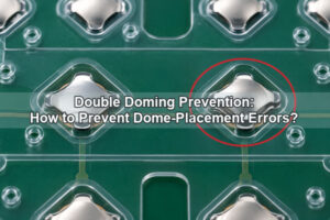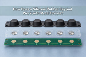

In tactile-switch design, a snap array means a snap dome array or metal dome array: multiple formed metal domes held in precise positions by an adhesive-backed PET carrier and installed over PCB, FPC or membrane-switch contacts. It reduces individual dome placement work, but reliable performance still depends on stack-up, dome geometry, pad support, venting, adhesive clearance, actuator alignment and assembly tolerance.

What Is a Snap Array?
A snap array is a pre-positioned sheet of stainless-steel snap domes. Each dome sits in a defined pocket or adhesive opening, and the complete sheet aligns with a set of normally open contacts on a circuit. Pressing a dome makes its center bridge the inner contact while its rim or legs remain on the outer contact, creating a momentary electrical closure. The dome returns when the load is removed.
The term is not as standardized as snap dome array, metal dome array or dome sheet. A drawing should therefore define the actual construction instead of relying on the name alone. The drawing needs to identify the carrier layers, dome part numbers, orientation, cutouts, vent paths, release liner and circuit-side reference.
How Does a Snap Array Work on a PCB?
The array controls mechanical location; the PCB completes the switch circuit. Each dome must seat on one flat outer contact plane and remain centered over an electrically isolated center pad. During actuation, the dome snaps through, touches the center pad and closes the circuit. On release, stored spring energy restores the dome and opens the contact.
The force path includes more than the metal dome. A keycap, graphic overlay or plunger transfers the load, the PET carrier retains the dome, the circuit pads provide electrical contact, and the PCB or enclosure supplies reaction support. A soft backing can absorb travel before snap-through. An off-center actuator can tilt the dome, causing inconsistent force, incomplete contact or early fatigue.
Which Snap Array Stack-Up Should You Choose?
Choose the simplest stack that provides accurate retention, a clear air path and enough environmental protection. A basic assembly may use one adhesive PET carrier over the domes. A more controlled construction adds a spacer below the carrier to define the cavity and connect vent channels. Other functional layers should be added only when the application needs them.
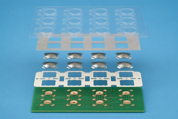
| Layer or feature | Primary function | Design control |
|---|---|---|
| Overlay or actuator | Transfers the user load | Centering, contact-face diameter, preload and hard stop |
| PET carrier | Holds domes at fixed X-Y positions | Thickness, stiffness, cutouts and dimensional stability |
| Pressure-sensitive adhesive | Bonds the array to the circuit | Clearance from dome feet, contacts and air channels |
| Metal dome | Provides snap action and electrical bridging | Shape, size, trip force, return force, travel and life |
| Spacer or cavity layer | Defines clearance and routes air | Cavity height, channel width and sealing boundary |
| PCB, FPC or membrane circuit | Provides contacts and signal routing | Pad geometry, flatness, finish and local support |
Additional options can include printed shielding, a rubber-glue interface, a light-guide film or a raised actuator. These features change thickness, force transfer and tolerance accumulation, so they should be released as part of the complete stack rather than added after dome selection.
How Do Single-Layer and Double-Layer Snap Arrays Differ?
The practical difference is cavity control. A single-layer construction is thin and direct, while a double-layer construction uses a spacer or lower adhesive layer to control clearance and air routing.
| Decision point | Single-layer array | Double-layer array |
|---|---|---|
| Structure | Domes retained beneath one adhesive PET carrier | Carrier plus spacer or lower layer around dome cavities |
| Best fit | Thin, straightforward layouts with controlled vent holes | Layouts needing defined air channels, added clearance or better underside protection |
| Main risk | Blocked vent or carrier interference if the cutout is too small | Excess stack height or misregistration between layers |
| Drawing focus | Dome pocket, vent hole and adhesive boundary | All single-layer controls plus cavity height and channel continuity |
A single-layer dome array is appropriate when each cavity can vent directly and the circuit provides a stable contact plane. A double-layer dome array is useful when the spacer must protect the carrier from dome edges, create connected air paths or improve dust control. More layers are not automatically better; they add alignment and thickness tolerances.
Which Dome Shape, Force, Travel and Size Should You Specify?
Start with the available key footprint and actuator geometry, then define the tactile targets. Round domes provide symmetric support. Four-leg domes create distinct support points and open sectors that can help with trace escape and venting. Triangle domes fit compact layouts, while oblong domes suit narrow or elongated keys. The pad pattern must match the selected dome family.
Do not specify trip force alone. Include return force or click ratio, travel, height, life requirement and acceptable tolerance. Metal-Domes publishes typical dome-array ranges of 0.28-0.45 mm total height, 0.13-0.30 mm travel, 100-400 gf force and more than one million cycles for applicable constructions. These are reference ranges, not universal guarantees; the released dome geometry and test method control the final values.
The actuator contact should remain near the dome center without creating a point load. When the housing cannot reach the dome cleanly, a plunger actuator dome array can add a controlled force-transfer feature. Its diameter, height, hardness, concentricity and maximum stroke must be included in the stack analysis.
How Should PCB Contact Pads and Vent Paths Be Designed?
The contact pattern must support the dome on one plane while keeping the center electrode isolated from the outer electrode. Every leg or rim segment should land on a stable conductive area. Raised vias, solder-mask steps, uneven plating or traces under a support point can tilt the dome and change the force-displacement response.
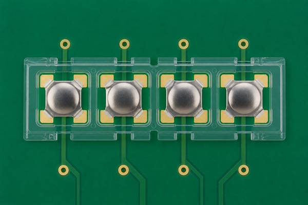
Air must leave the cavity when the dome is pressed and return when it releases. The route may pass through open sectors around a four-leg dome, a die-cut spacer channel or a dedicated vent hole. It must remain open after lamination and should not terminate under adhesive, inside a liquid trap or at a contamination source. Connected cavities also need review because one key can influence the pressure beneath another.
The detailed PCB contact pad design for metal dome switches should be checked together with the array drawing. The circuit and carrier need common datums so that copper, coverlay or solder-mask openings, dome pockets and vent channels share one tolerance scheme.
How Are Snap Arrays Aligned and Laminated?
Alignment should reference functional circuit features, not only the outer board edge. Tooling holes, optical targets or fiducials should establish the relationship between the dome centers and contact pads. The array is peeled from its release liner, aligned without stretching the carrier, and laminated through a supported fixture that does not accidentally actuate the domes.
- Clean and inspect the contact surface before lamination.
- Use at least two separated registration features to control translation and rotation.
- Keep adhesive clear of dome support points, center contacts and vent paths.
- Support the PCB or FPC beneath every active key during lamination.
- Inspect dome position, film wrinkles, trapped particles and channel continuity afterward.
Do not pull the PET sheet into alignment after one side has bonded. Carrier tension can preload domes and create key-to-key variation. If the assembly has many keys or tight registration, a placement fixture and pilot run are usually more reliable than manual visual alignment.
What Materials and Adhesives Affect Reliability?
The carrier, adhesive, spacer, circuit finish and enclosure support all influence reliability. PET is common because it is thin and dimensionally stable, but its thickness and stiffness affect how the sheet follows local steps. The adhesive must bond to the actual circuit surface over the expected temperature and humidity range without creeping into the dome cavity.
Selection should consider substrate surface energy, operating temperature, humidity, chemical exposure, expected storage time and rework policy. A stronger adhesive is not always safer: excessive flow or squeeze-out can block vents, contaminate contacts or restrict dome movement. The dome array adhesive selection should therefore be evaluated with the cavity geometry and process pressure.
What Common Snap Array Failures Should Be Prevented?
Most failures come from an interface mismatch rather than the stainless-steel dome alone. The symptom should be traced through the complete force path and electrical path.
| Symptom | Likely cause | Corrective direction |
|---|---|---|
| High or inconsistent trip force | Blocked vent, tilted dome, flexible backing or carrier preload | Restore airflow, support the circuit and correct registration |
| Intermittent electrical closure | Contamination, uneven pad finish, off-center dome or insufficient travel | Control cleanliness, flatness, centering and actuator stroke |
| Slow or incomplete return | Adhesive intrusion, excess preload or trapped cavity pressure | Increase functional clearance and verify the vent path |
| Key-to-key feel variation | Layer misregistration, different support conditions or actuator variation | Use shared datums, common fixtures and an assembly-level test |
| Carrier damage near a dome edge | Insufficient pocket clearance, burr orientation or repeated over-travel | Review cavity geometry, dome condition and the mechanical hard stop |
Over-travel deserves a mechanical stop in the enclosure or actuator. Using the dome as the hard stop can permanently deform it, reduce return force or shorten life even when the switch still clicks during early testing.
Which Tests Should Validate a Snap Array?
Validation should measure the finished switch stack, not only loose domes. The same array can feel different on a rigid fixture, unsupported FPC or production housing. Fixtures, probe diameter, test speed, support condition and electrical threshold should be documented so results can be compared.

- Force-displacement testing records trip force, return force, travel and click ratio.
- Continuity or contact-resistance testing verifies make and break at defined positions.
- Optical inspection checks dome centering, carrier damage, adhesive intrusion and contamination.
- Life cycling tracks force, travel and resistance changes over the required actuation count.
- Temperature and humidity testing evaluates adhesive movement, dimensional change and corrosion risk.
- Assembly trials verify peel behavior, fixture alignment, lamination repeatability and final key feel.
What Information Should Be Released for Production?
A production package should remove ambiguity from both the mechanical stack and the tactile target. At minimum, release the array outline, datum scheme, dome coordinates and orientation, circuit contact drawing, vent layout, layer stack, adhesive boundaries, release-liner direction and inspection requirements.
- 2D drawing with overall dimensions, cutouts, tooling holes and tolerances
- PCB, FPC or membrane contact layout with common datums
- Dome shape, size, part number, trip force, travel and life target
- Carrier, spacer, adhesive and optional functional-layer requirements
- Actuator contact diameter, preload, maximum stroke and support condition
- Operating temperature, humidity, sealing and chemical exposure
- Prototype quantity, production quantity and required test records
A custom dome array can combine different dome sizes, shapes or forces on one carrier when the drawing defines each position. EBest Circuit(Best Technology) has manufactured metal domes and dome arrays since 2006 and can review AutoCAD, PDF, Gerber, PCB/CAM files or customer drawings. Final capability still depends on dome geometry, array stack-up, adhesive, circuit layout and the agreed test method.
FAQ
Is a snap array the same as a snap dome array?
In metal-dome projects, the terms are often used for the same product concept. Because snap array is ambiguous in other industries, drawings and purchase documents should use snap dome array or metal dome array and define the layer structure.
Can a snap array be installed on FPC?
Yes. The active key area needs a stable support or stiffener, and the bend zone should stay away from dome footprints, spacer edges and contact pads. Coverlay openings and array datums must align with the copper pattern.
Does every dome cavity need a vent?
Every cavity needs a reliable route for air movement. The route may be an individual hole or a connected spacer channel, but it must remain open after lamination and under the final enclosure.
Can different dome forces be used on one array?
Yes, provided each position is identified in the drawing and the actuator and pad geometry support the selected dome. Mixed force does not remove the need to control return force, travel and tolerance.
Should a snap array use single-layer or double-layer construction?
Use single-layer construction for thin, straightforward layouts with reliable direct venting. Use double-layer construction when a spacer is needed to define cavities, route air or protect the carrier. The final choice should follow the complete stack and environment.
What causes inconsistent tactile feel across an array?
Common causes are uneven PCB support, off-center actuators, blocked vents, dome misalignment, carrier tension, adhesive intrusion and variation in actuator stroke. Testing the final assembly is the fastest way to separate dome variation from stack variation.
Conclusion
A successful snap array is designed as a complete switch stack. Select the layer structure and dome geometry together, keep every contact and support point coplanar, provide a verified vent path, align the carrier to functional circuit datums and validate force and electrical behavior in the intended enclosure. For engineering review, prototype support or production discussion, email sales@metal-domes.com or use the Metal Dome and Dome Array contact page.