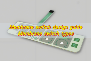
What Is Membrane Switch PCB Design?
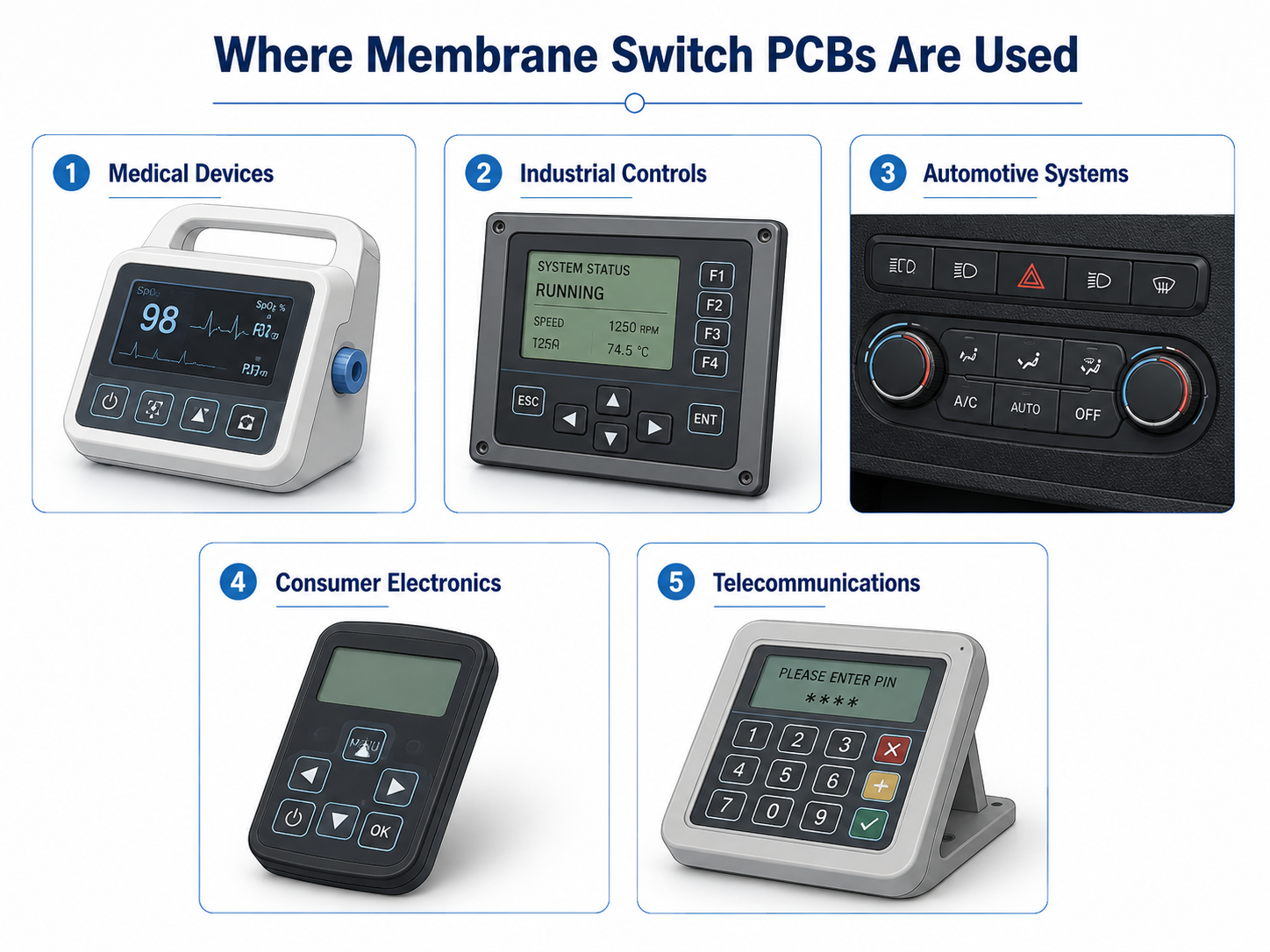
A membrane switch PCB design combines a printed circuit board with a membrane switch structure to create a compact and reliable user interface. It is widely used in medical devices, industrial controllers, consumer electronics, automotive systems, and communication equipment.
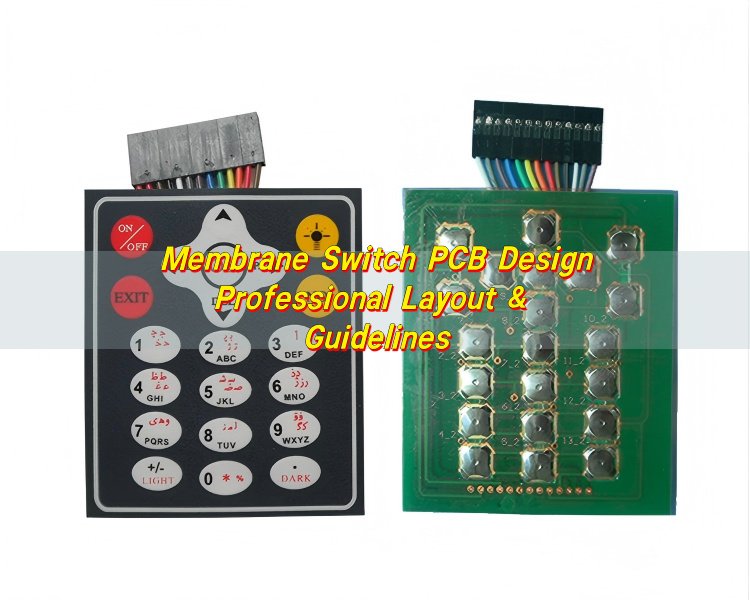
Unlike traditional mechanical buttons, membrane switch structures are thinner, easier to seal against dust and moisture, and more flexible for custom layouts. The PCB works together with overlays, adhesive layers, metal domes, LEDs, and connectors to create stable electrical switching and tactile feedback.
At EBest Circuit (Best Technology), membrane switch PCB projects are commonly designed for applications that require compact structures, stable switching, and long operating life.
Typical membrane switch structures include:
- Graphic overlay
- Adhesive spacer
- Metal dome or conductive contact
- PCB contact pads
- LED backlighting
- Connector tail
Common applications include:
| Industry | Application |
|---|---|
| Medical | Diagnostic equipment |
| Industrial | Control panels |
| Automotive | Dashboard controls |
| Consumer Electronics | Portable devices |
| Telecommunications | Keypad systems |
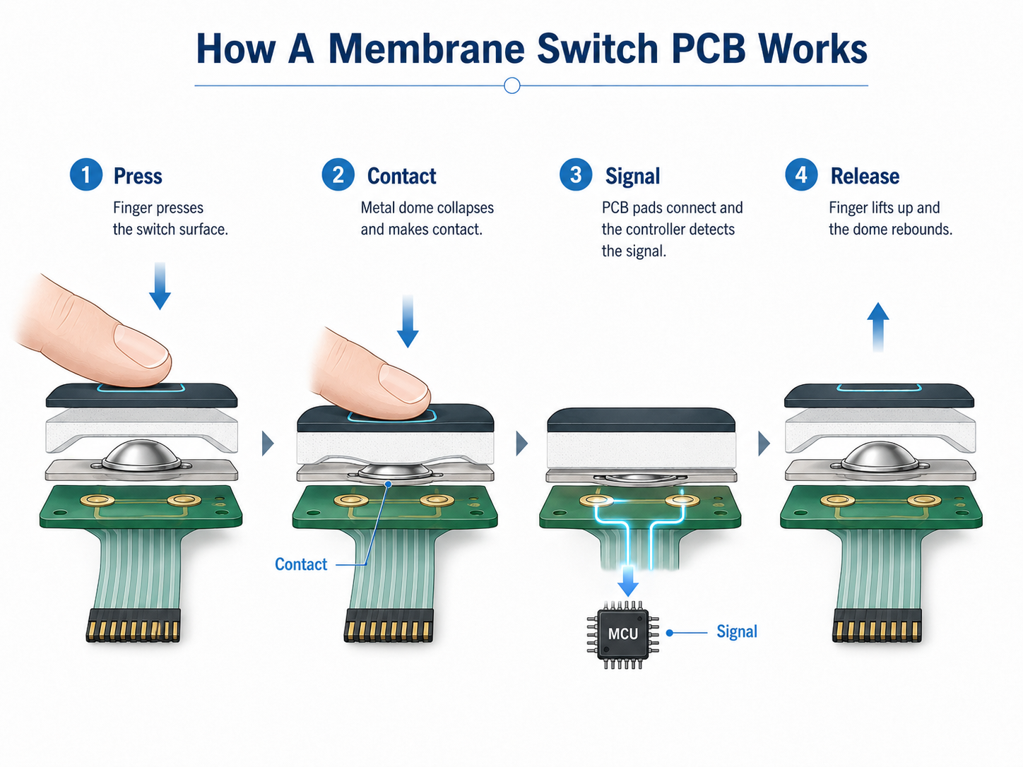
How Does a Membrane Switch PCB Work?
A membrane switch PCB works by creating an electrical connection when pressure is applied to the switch area. In metal dome designs, pressing the surface collapses the dome and connects the PCB contact pads. When the pressure is released, the dome returns to its original shape and disconnects the circuit.
Basic switching process:
- User presses the switch surface.
- The dome contacts the PCB pads.
- The controller detects the signal.
- The dome rebounds after release.
PCB layout directly affects switch performance. Pad geometry, trace routing, and solder mask clearance all influence tactile response and electrical stability.
Common contact pad structures include:
| Pad Style | Purpose |
|---|---|
| Circular ring | Smooth contact |
| Four-leg pattern | Stable switching |
| Cross pattern | Balanced force distribution |
Compared with mechanical buttons, membrane switch PCBs provide:
| Feature | Membrane Switch PCB | Mechanical Button |
|---|---|---|
| Thickness | Thin | Thicker |
| Waterproofing | Better | Moderate |
| Layout Flexibility | High | Limited |
| Cleaning Resistance | Strong | Moderate |
When Should You Use a Membrane Switch PCB?
Membrane switch PCBs are suitable for products that require:
- Thin structures
- Sealed surfaces
- Long operating life
- Lightweight construction
- Integrated backlighting
- Custom keypad layouts
These designs are commonly used in environments exposed to dust, moisture, vibration, or frequent cleaning.
Typical applications include:
| Product Type | Example |
|---|---|
| Medical devices | Portable analyzers |
| Industrial equipment | Machine controllers |
| Automotive systems | HVAC panels |
| Consumer electronics | Handheld terminals |
| Security systems | Access keypads |
Membrane switch structures also simplify assembly in medium- and high-volume production because multiple keys can be integrated into a single interface layer.
What Should Be Included in a Membrane Switch Design Guide?
A membrane switch design guide should define both electrical and mechanical requirements.
Important design considerations include:
- PCB layout
- Contact pad dimensions
- Dome alignment
- Trace routing
- LED placement
- Connector structure
- Material selection
- Adhesive specifications
- Environmental protection
Switch spacing is important for reliable operation. Keys placed too closely may affect usability and structural stability.
Typical actuation force ranges:
| Application | Typical Force |
|---|---|
| Consumer electronics | 160–250 gf |
| Medical devices | 180–300 gf |
| Industrial controls | 250–450 gf |
| Automotive systems | 300–500 gf |
LED integration guidelines should also define:
- LED spacing
- Diffuser placement
- Brightness uniformity
- Light leakage control
ESD protection and grounding design are also necessary in user-operated products.
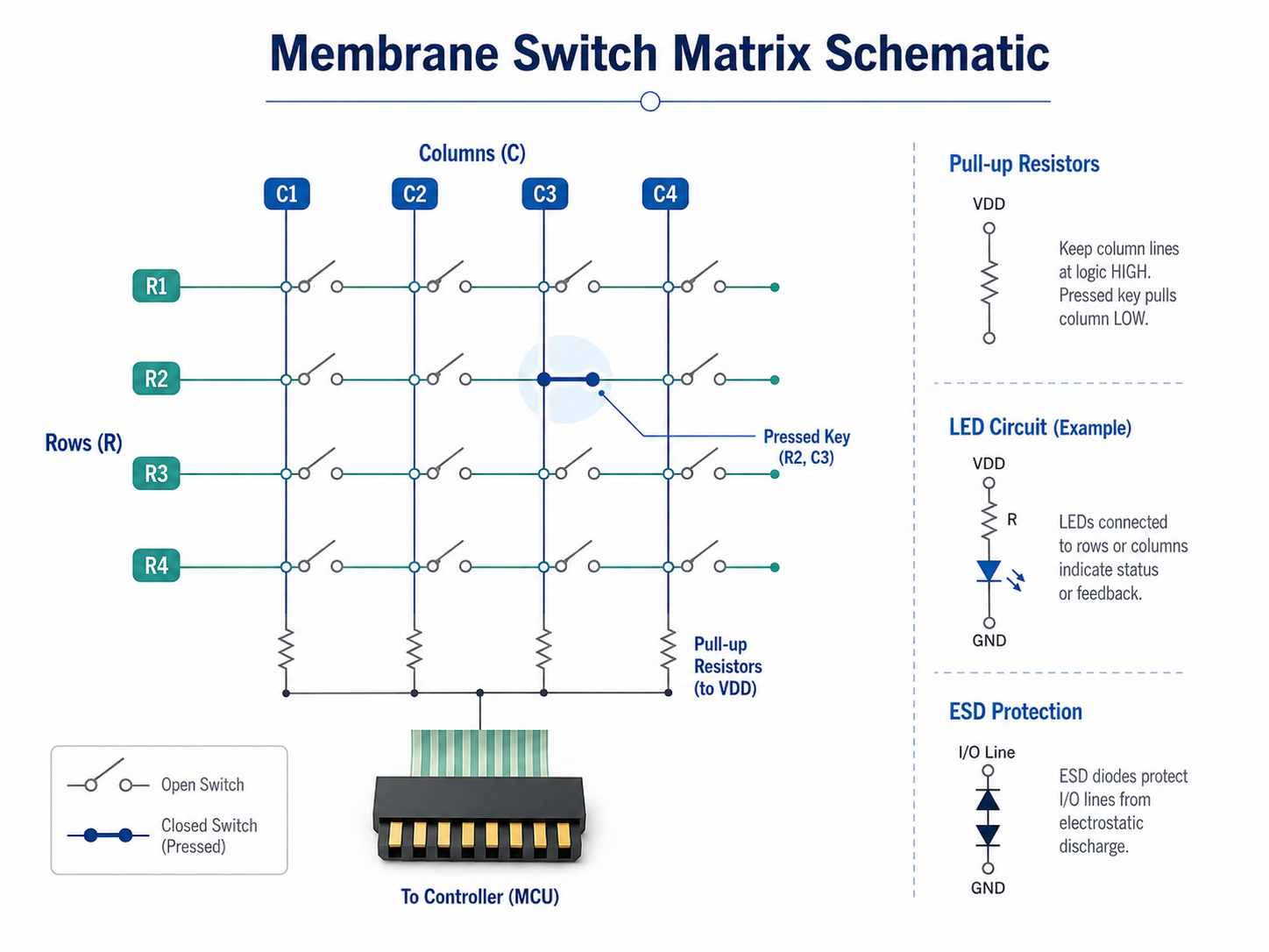
How Do You Create a Membrane Switch Schematic?
A membrane switch schematic defines the electrical connection between the switch matrix and the controller. Most membrane switch systems use matrix circuits to reduce trace count and connector size.
Basic matrix structure:
- Rows carry scan signals
- Columns detect switch activation
- Pressing a key bridges a row and column
Typical schematic elements include:
- Switch matrix
- LED circuits
- ESD protection
- Pull-up resistors
- Connector pin assignments
- Ground routing
Comparison of wiring methods:
| Feature | Direct Wiring | Matrix Wiring |
|---|---|---|
| Trace Count | Higher | Lower |
| Connector Size | Larger | Smaller |
| Circuit Complexity | Lower | Moderate |
| Suitable For | Small keypads | Large keypads |
Long flexible tails require careful routing to prevent signal instability or voltage drop.
What Does a Membrane Switch Diagram Show?
A membrane switch diagram illustrates the physical structure of the switch assembly. Unlike schematics, diagrams focus on layer arrangement and component placement.
Typical diagram contents include:
- Overlay structure
- Spacer openings
- Dome locations
- PCB contact pads
- LED positions
- Connector areas
- Alignment holes
These diagrams help identify layout conflicts before production.
Common diagram elements:
| Diagram Element | Function |
|---|---|
| Dome center marks | Alignment |
| Spacer openings | Dome movement |
| LED windows | Light transmission |
| Adhesive zones | Layer bonding |
| Contact pads | Electrical switching |
3D previews are often used to verify lighting distribution and switch alignment before manufacturing.
What PCB Materials Are Used for Membrane Switches?
Material selection affects flexibility, durability, and electrical performance.
Common PCB materials include:
- FR4 rigid PCB
- Flexible polyimide PCB
- PET circuits
- Aluminum-backed PCB
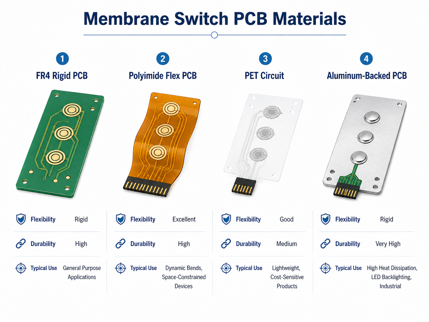
Material comparison:
| Material | Flexibility | Durability | Typical Use |
|---|---|---|---|
| FR4 | Low | High | Industrial panels |
| Polyimide Flex PCB | High | High | Compact electronics |
| PET Circuit | Very High | Moderate | Consumer keypads |
| Aluminum PCB | Low | Very High | LED systems |
Common surface finishes include:
- ENIG
- Carbon ink
- Immersion silver
- OSP
ENIG is widely used because it provides stable contact performance and corrosion resistance.
At EBest Circuit (Best Technology), ENIG surface treatment is commonly used in membrane switch PCB manufacturing for stable dome contact performance.
How Should Contact Pads Be Designed for Stable Switching?
Contact pad design directly affects tactile consistency and electrical reliability.
Key design factors include:
- Pad diameter
- Gap spacing
- Surface finish
- Solder mask clearance
- Copper thickness
- Dome alignment
Common contact pad styles:
| Pad Style | Advantage |
|---|---|
| Four-leg pattern | Stable contact |
| Circular ring | Smooth tactile feel |
| Cross pattern | Balanced switching |
| Carbon contact | Lower wear |
Poor solder mask control may cause inconsistent dome movement or unstable switching. Most designs maintain tight alignment tolerances to ensure consistent actuation across all keys. Environmental conditions should also influence pad design choices, especially in humid or contaminated environments.
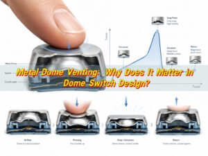
How Do Metal Domes Affect Membrane Switch Design?
Metal domes determine tactile response, actuation force, and switch lifespan. When pressed, the dome collapses and connects the PCB pads. After release, it returns to its original shape.
Common dome types:
| Dome Type | Characteristics |
|---|---|
| Four-leg dome | Stable contact |
| Triangle dome | Strong tactile snap |
| Round dome | Smooth actuation |
| Oblong dome | Narrow layouts |
Important dome selection factors include:
- Snap ratio
- Actuation force
- Lifecycle rating
- Dome height
- Electrical resistance
Typical dome lifespans:
| Dome Material | Lifecycle |
|---|---|
| Stainless steel | 1–5 million cycles |
| Nickel-plated dome | 500k–2 million cycles |
| Gold-plated dome | Improved conductivity stability |
Common dome mounting methods include:
- Adhesive dome arrays
- Individual placement
- Polyimide carrier films
At EBest Circuit (Best Technology), custom dome array integration is optimized together with PCB pad design to improve switching consistency during mass production.
How Should LED Backlighting Be Designed in a Membrane Switch PCB?
LED backlighting improves visibility and supports operation in low-light environments.
Proper LED integration requires attention to:
- LED position
- Brightness uniformity
- Heat management
- Light diffusion
- Power consumption
Common backlighting methods:
| Backlighting Type | Typical Application |
|---|---|
| SMT LED | Industrial panels |
| Light guide film | Consumer electronics |
| Fiber optic | Automotive systems |
| EL panel | Thin interfaces |
Poor LED placement may create uneven brightness or light leakage.
Thermal management is also important in high-brightness designs. Excessive heat may reduce adhesive stability or LED lifespan.
Common thermal control methods include:
- Low-power LEDs
- Copper heat spreading
- Thermal vias
- Optimized duty cycles
White LEDs are commonly used because they provide clear visibility through membrane overlays.
In summary, membrane switch PCB design combines electrical layout, tactile structure, material selection, and lighting integration into a single interface system. Proper PCB design improves switching consistency, assembly reliability, and operational lifespan. For membrane switch PCB support or technical consultation, contact sales@metal-domes.com