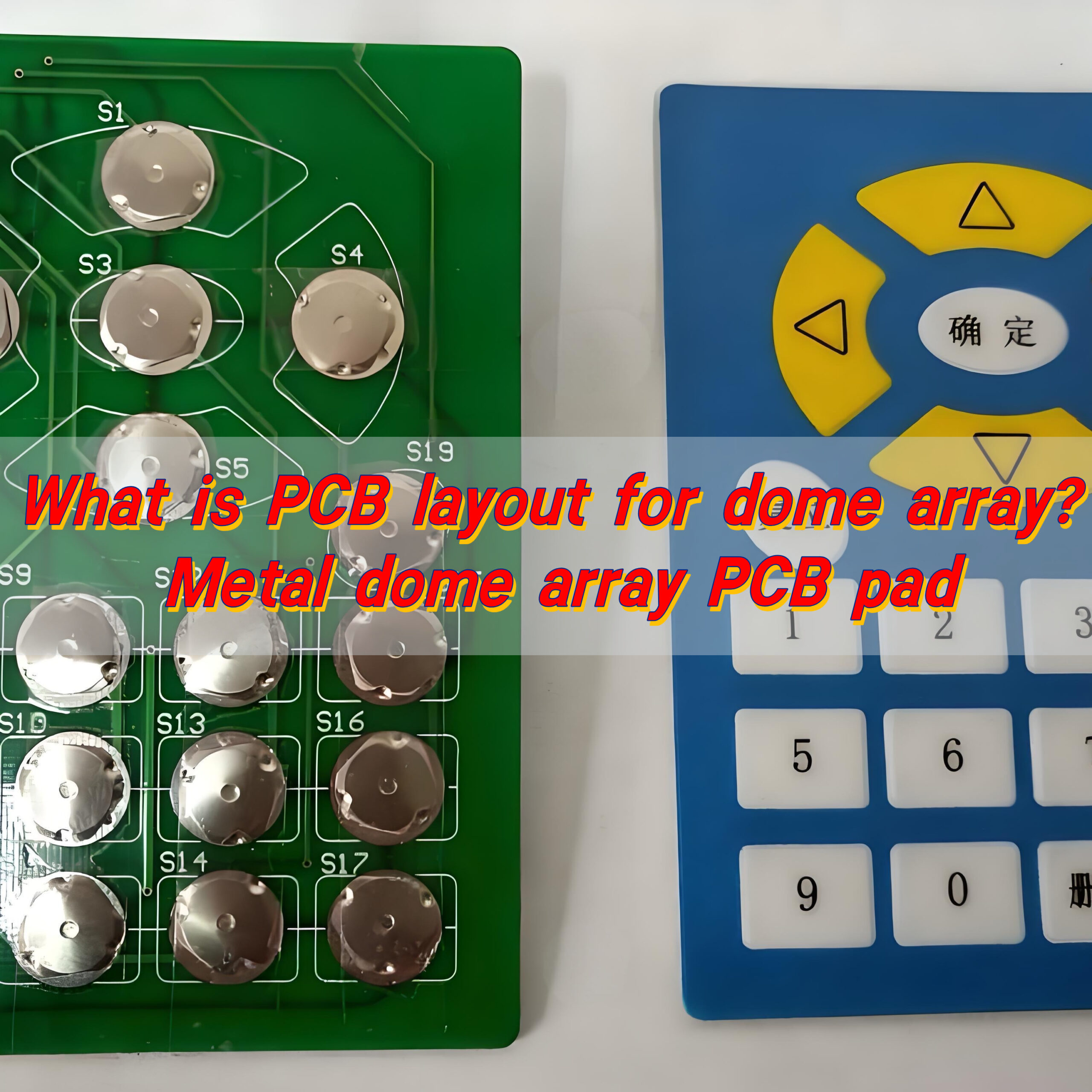
PCB layout for dome array is the design pattern on a circuit board that defines where each metal dome sits and connects electrically. When pressed, the dome bridges two pads to send a signal. This layout ensures accurate alignment, stable contact, and consistent tactile feel.
What is PCB for Metal Dome Array?
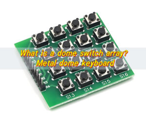
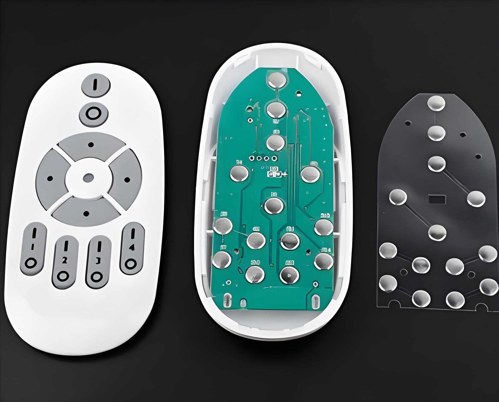
A PCB for metal dome array is a printed circuit board specifically designed to integrate with metal domes used as tactile switches. These domes act as tiny momentary contacts that bridge two pads on the PCB when pressed, sending a signal to the circuit.

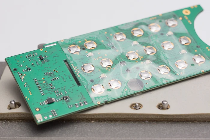
Each dome sits on a dedicated PCB pad, often covered with a spacer or overlay to ensure proper tactile feedback. The board material, surface finish, and trace routing all influence how well the dome performs. A clean, smooth pad surface provides stable conductivity, while the correct dome placement ensures uniform tactile feel across every key.
What is a PCB Dome Array Used For?
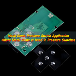
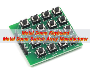
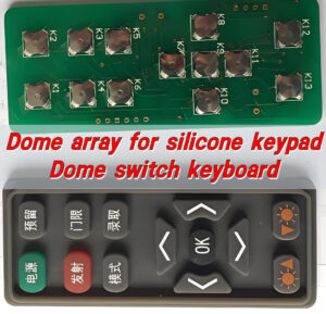
A PCB dome array is widely used in applications that demand precise tactile response and compact design. You’ll find it in devices such as industrial control panels, telecom equipment, medical devices, and consumer electronics.
Each dome in the array acts as a tiny switch. When pressed, it snaps to complete the circuit, then returns to its original shape after release. This snap action gives users a satisfying click and reliable feedback. Because of its simplicity, the metal dome switch array outlasts many traditional button mechanisms and offers cleaner electrical contact.
In high-volume products, such as remote controls or handheld instruments, the PCB dome array also helps reduce manufacturing costs. The array design simplifies alignment, reduces soldering steps, and ensures consistent actuation across the board.
Which PCB Suits a Metal Dome Switch Array Best?
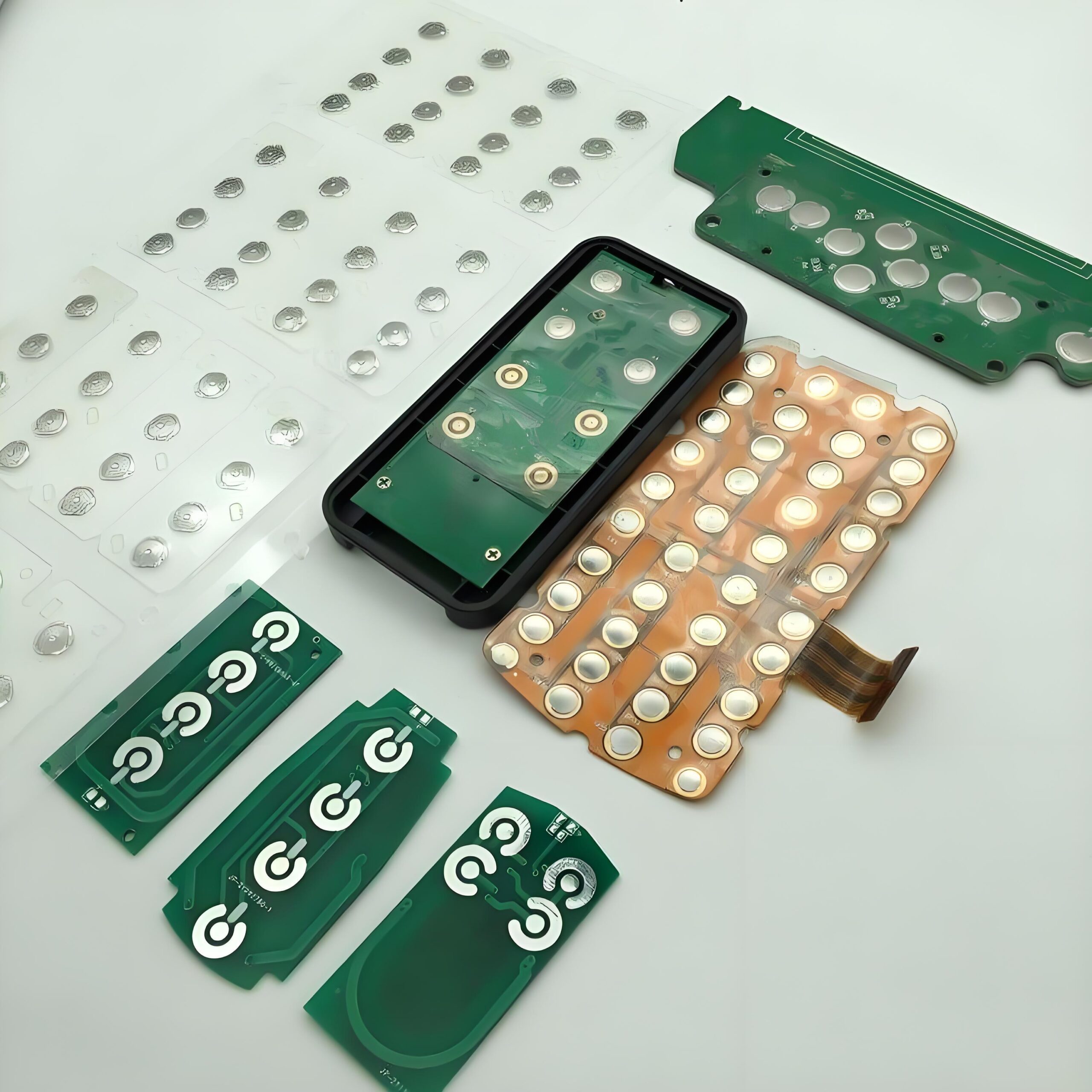
Choosing the right PCB for a metal dome switch array requires a balance between durability, electrical stability, and tactile performance. FR4, PET, and flexible polyimide are the most common materials used for dome switch PCBs.
FR4 PCB is the standard choice for rigid designs. It’s strong, dimensionally stable, and cost-effective. This makes it ideal for devices where the keypad area doesn’t flex during use. The metal domes adhere directly to the PCB pads, protected by an overlay or adhesive sheet.
Flexible PCB (FPC), often made from polyimide, works best for curved or space-limited designs. It allows the metal dome array on PCB to follow non-flat surfaces while maintaining strong electrical connections. Flex PCBs also reduce assembly steps, as they can connect directly to other circuits without extra connectors.
PET-based PCBs are commonly used in lightweight or disposable applications. They offer a balance between flexibility and cost, making them suitable for consumer electronics or medical instruments that require compact tactile panels.
No matter the material, the key is smooth pad surface and tight tolerance. The metal dome array PCB pad must align perfectly with the dome to ensure consistent actuation and prevent false triggers. Proper surface treatment, such as ENIG (Electroless Nickel Immersion Gold), enhances conductivity and corrosion resistance, keeping the switch stable over millions of cycles.
Can PCB for Metal Dome Array Be Customized?
Absolutely. The PCB for metal dome array is highly customizable, both in electrical layout and mechanical structure. Since every product has different functional and aesthetic needs, customization is often the best way to achieve optimal tactile performance.
You can customize parameters such as:
- Pad shape and size: Circular, cross, or rectangular patterns can be used depending on dome type.
- Trace routing: Ensures minimal resistance and clean signal transmission.
- Pad finish: ENIG or hard gold finishes maintain high reliability.
- Board thickness: Determines flexibility and tactile consistency.
- Mounting position: Dome alignment must match graphic overlay or button icons.
Customization also extends to dome types. For example, you might choose four-leg domes for precise centering or triangle domes for compact designs. A metal dome switch array can also include domes with different actuation forces to match various functions on a single panel.
Modern PCB manufacturers, like Best Technology, use advanced SMT and laser-cutting techniques to achieve pad accuracy within ±0.05 mm. This precision ensures perfect contact and repeatable tactile feedback across every key position.
What Matters Most in PCB Array Design?
Designing a PCB array for metal domes demands attention to several critical factors. Each influences how well the switch performs and how long it lasts.
- 1. Pad Alignment and Geometry
The pad layout defines where and how the dome contacts. Pads should be symmetrically designed with clean edges and proper spacing to prevent short circuits.
- 2. Surface Finish
Smooth and corrosion-resistant finishes like ENIG improve contact reliability. Avoid rough or oxidized surfaces that can degrade dome performance.
- 3. Dome Centering
Every dome must be centered precisely over its pad. This ensures consistent tactile feel and reduces mechanical wear. Automated placement through Tape & Reel packaging is a great solution to maintain accuracy in mass production.
- 4. Trace Design
Keep traces short and balanced to minimize resistance. Avoid routing under domes unless necessary. Balanced trace lengths ensure even signal response.
- 5. Spacer and Overlay
The spacer layer isolates domes while maintaining their position. The overlay provides the tactile surface that users press.
- 6. Ground and Shielding
Adding a ground plane helps minimize noise, especially in sensitive circuits. Proper shielding prevents false triggers from EMI.
How to Design a PCB Layout for Dome Arrays?
Designing a PCB layout for dome array begins with understanding how domes interact with circuit pads. Each dome acts as a bridge, closing the contact when pressed.
Start with defining your array configuration. Decide how many domes your panel requires and their arrangement. Then, determine the pad diameter and spacing. For most domes, pad diameters range from 3 to 12 mm depending on actuation force and dome size.
When creating the pad pattern:
- Use clean, round edges to ensure proper contact.
- Avoid sharp corners that may trap air or cause uneven adhesion.
- Keep uniform spacing between adjacent domes to avoid interference.
- Next, design the circuit traces. Route them efficiently to each dome pad, avoiding unnecessary loops. Where multiple domes connect to a common ground, use short traces to reduce resistance.
- For assembly, include alignment marks and fiducials on the PCB. These help automatic pick-and-place machines position domes precisely. If using Tape & Reel metal domes, this ensures rapid and accurate mounting at speeds up to 100,000 domes per hour.
- Lastly, simulate your layout. Run continuity and short tests before production. PCB simulation software can verify that the metal dome array on PCB will function as intended under different conditions.
How to Place a Metal Dome Array on a PCB Pad?
Placing a metal dome array on PCB is a delicate process that affects switch quality and product life.
For single domes, manual placement is sometimes possible for prototypes or small batches. However, for large-scale production, Tape & Reel packaging offers major advantages. Each dome is pre-positioned on a tape and automatically picked by SMT machines, ensuring high speed and accuracy. The domes are placed directly onto their PCB pads with precise centering and correct orientation.
Here’s how the placement process typically works:
- Clean the PCB surface to remove dust or oil.
- Align domes using fiducial marks or optical systems.
- Apply adhesive layer or array sheet over the domes to fix them in place.
- Perform pressing test to confirm tactile feel and continuity.
- Add overlay layer for user interface and protection.
Maintaining clean conditions during placement is essential. Even tiny particles can affect dome contact. After placement, electrical testing ensures each dome makes stable contact without resistance fluctuation.
How to Improve Metal Dome Array PCB Pad Design?
Improving the metal dome array PCB pad design means optimizing for durability, sensitivity, and manufacturability. Here are some practical ways to enhance your pad design:
- 1. Optimize Pad Surface Finish
Use ENIG or hard gold plating. These finishes maintain high conductivity and prevent oxidation.
- 2. Refine Pad Geometry
Adjust pad diameter to match dome size precisely. The contact area should be large enough for stable signal but not so wide that it weakens the tactile response.
- 3. Ensure Centered Contact
Offset domes or misaligned pads lead to uneven clicking force.
- 4. Control Adhesive Thickness
Too much adhesive under the dome can reduce sensitivity. Too little can cause air pockets.
- 5. Add Vias and Ground Shield
For high-speed or noisy environments, grounding improves signal stability.
- 6. Choose High-Quality Domes
Select domes with consistent actuation force and precise shape.
- 7. Conduct Environmental Testing
Test your PCB dome array under temperature, humidity, and vibration. This ensures your design performs well in real-world conditions.
Conclusion:
PCB layout for dome array combines electrical precision with mechanical harmony. Every trace, pad, and dome must align perfectly to deliver fast response, stable contact, and pleasant tactile feel.
With optimized layout and materials, your metal dome switch array will deliver outstanding feel and durability across millions of presses. Contact: sales@metal-domes.com